Hida•2018-06-04• The more viable way forward for cutting-edge technology at the moment is to merge optical and semiconductor processes, and to use semiconductor thinking to make nanoscale optical components
Wafer-level optical technology now makes possible a range of new cutting-edge requirements, including 3D imaging and face recognition, AR MR, 5G optical communications, smart industry, and more Even some popular electrical fields, perhaps
Shangguan 2018-07-09 07:44:52 Last year, the Shanghai municipal government included silicon photonics in the first batch of major municipal special projects,
New Beijing News (Reporter Cai Haoshang) May 7, focusing on wafer-level optical chip company KunYou Optoelectronics announced the completion of the A2 round of financing, this round by Yuan Jing Capital, Huadeng International and the Chine
36 Krypton 2017-12-2936 Krypton has learned that KunYou Optoelectronics has recently completed a new round of financing, followed by KunZhong Capital, Sunny Optical, as well as the previous round of investment institutions in the Hengxingguang, ChenHui Ve
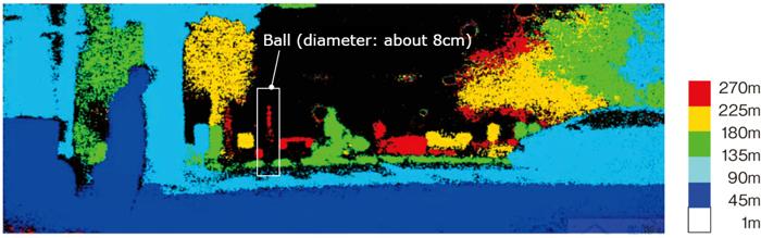
Gaijin Auto 2018-08-17 06:47:45 Gaijin Auto News According to foreign media reports, Japan s Panasonic Corporation (Panasonic Corp) has developed a depth image sensor (range image sensor)
Sina VR2018-10-09 20:01:06 In the last most hardcore experience and technical analysis, in-depth comparison of Magic Leap One and HoloLens article, AR hardware The chief scientist of software company Rave K
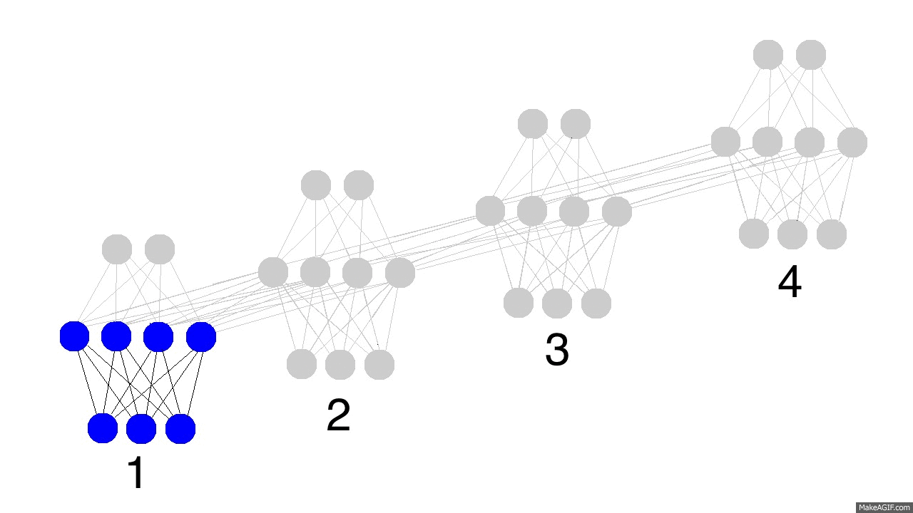
From techcrunch, by Devin Coldewey, compiled by Machine Mind Signals between neurons in the brain travel at about 100 meters per second, while light travels at 300,000 kilometers per second
Originally screened on VR2018-07-18 08:12:0110 members shared their thoughts on the impact of Apple s wireless headset on the AR VR market, as well as on Apple itself (screened on July 18, 2018)