In micro/nano optics, the precision of structural components imposes extremely strict requirements on the fabrication process. At the same time, different morphologies, feature sizes, and materials impose varying demands on the fabrication techniques. North Ocean Photonics possesses world-class fabrication equipment and processes that can meet diverse high-precision fabrication and master processing requirements. The company offers a variety of custom master services for customers:
1. Size Options: From samples of a few square millimeters to standard 6-inch, 8-inch, and 12-inch wafers.
2. Material Options: Offering a range of materials including silicon wafers, SOI, glass, quartz, silicon carbide, lithium niobate, and polymers.
3. Process Options: Depending on customer precision, time, and cost requirements, a variety of choices are provided, including electron beam lithography, etching, laser direct writing, and large-scale integrated circuit processes, achieving feature sizes from 10 nm to several hundred micrometers, from single-layer structures to multi-layer (8-layer, 16-layer, etc.) and complex continuous morphologies.
Based on customers' post-processing requirements, North Ocean Photonics also offers customized master processing services, including master sputtering, master to metal plate conversion (e.g., nickel plates), and anti-sticking treatments.
The fabrication techniques provided by North Ocean Photonics include:
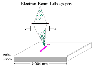
Electron Beam Processing
Electron beam (eBeam) processing technology focuses an electron beam into a fine beam using electromagnetic fields to irradiate photoresists. Because the electron beam can be easily deflected and scanned by electromagnetic fields, complex patterns can be directly written onto the photosensitive film without the need for a mask. Compared to other lithography techniques, the advantages of electron beam lithography are significant: first, it offers high resolution, reaching tens of nanometers, and can achieve etching resolutions of a few nanometers. Second, electron beam lithography does not require masks, making it very flexible and suitable for small-scale, prototyping, and process validation during special periods.
Through electron beam technology, North Ocean Photonics can provide customers with master processing at extremely high resolutions (tens of nanometers). Considering factors such as precision, time consumption, and cost, North Ocean typically uses electron beam technology for prototyping services, allowing for efficient design verification and multiple iterations with short delivery times.
Ion Beam Processing
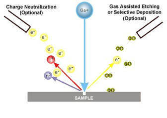
Ion beam lithography includes focused ion beam exposure (FIB), mask ion beam lithography (MIB), and ion beam sputtering lithography (IBP). Ion beam lithography uses an ion source for exposure. Its small emission area allows for easy focusing of emitted ions into a fine ion beam for high-resolution exposure. Focused ion beam exposure has some notable advantages compared to electron beam exposure: 1) Proximity effects can be neglected because ions are much heavier than electrons. Electrons have low mass, resulting in a larger scattering range in the resist, affecting the exposure quality of adjacent circuits; 2) The sensitivity of photoresists to ion beams is hundreds of times higher than that to electron beams. However, focused ion beam exposure has some drawbacks: 1) Its resolution is lower than that of electron beams due to the energy dispersion of ions, which limits focusing; 2) Ions have larger mass, resulting in a smaller exposure depth in the photoresist.
Through ion beam technology, North Ocean Photonics can provide the processing of fine gratings and special tooth-shaped grating masters. For specific processing requirements, please feel free to inquire.
Laser Direct Writing
Laser direct writing utilizes a variable intensity laser beam to expose the resist material on the substrate surface, creating the desired relief profile after development. The basic working principle of the laser direct writing system involves computer-controlled high-precision laser beam scanning that directly writes patterns onto the photoresist, transferring the patterns to the mask. North Ocean Photonics has a laser direct writing lithography line. Through laser direct writing and its organic integration with other processes (such as VLSI processes), North Ocean Photonics can achieve large-area, high-precision mask fabrication, multi-step two-dimensional grating processing, high aspect ratio spherical and aspherical arrays, and the fabrication of 3D micro-nano morphologies like compound eyes.
Single-Point Diamond Machining
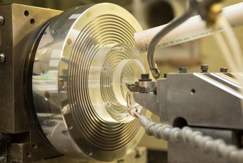
Single-point diamond machining technology uses precision CNC lathes and natural single-crystal diamonds as cutting tools, processed under computer control. Due to the high hardness, strong wear resistance, and excellent thermal conductivity of diamonds, the cutting edges can be extremely sharp (with edge radii less than 0.05 microns or even smaller). Single-point diamond machining is suitable for optical lenses, freeform surfaces, and large-scale (>100 microns) spherical and aspherical array processing.