
上观 2018-07-09 07:44:52

Last year, the Shanghai Municipal Government will be included in the first batch of silicon photonics municipal major special projects, invested a lot of money, the layout of silicon-based optical interconnect chip R & D and production. Now, many industry insiders sigh, Shanghai is really proactive, because the silicon-based optical interconnect chip is a new generation of communication chips, domestic communications companies have been stuck on the neck of this device.
Reporters recently learned from the Municipal Science and Technology Commission, Zhangjiang Laboratory led by the silicon photonics municipal major special projects in the process technology breakthroughs, with the ability to flow optical chip. Expected this year, China's first silicon photonics R & D pilot line will be built in Shanghai. This special project aims to build a silicon photonics chip industry chain in Shanghai, master the key core technologies, so that domestic enterprises to get rid of the dependence on foreign optical chip suppliers.
Building a global silicon photonics R&D center
Silicon photon municipal major special technology leader, Shanghai Institute of Microsystems and Information Technology, Chinese Academy of Sciences, researcher Yu Mingbin, optical chip in the global boom, is gradually replacing the traditional electric chip, becoming the mainstream of communication chips. In the chip between the square inches, electric transmission why will be replaced by optical transmission? He explained that a large number of electrons in the movement of high-density circuits, will make the device heat, but also produce electromagnetic losses, which affects the chip's speed, power consumption and other performance. Compared with it, the movement of light to & ldquo; light & rdquo; much more & mdash; & mdash; speed of the universe's fastest, the movement does not produce heat, and more light can be in the same time and space in the movement and to maintain their independence, thus significantly saving the signal transmission channel.
Because of the superior physical properties of light, in the field of communications, fiber optic cables are replacing cables; optical chips have also begun to replace the electric chip, in the silicon-based materials to achieve the transmission of optical signals. At present, the industrialization of optical chips is still in the early stages, optical chip suppliers in the world only a few, all in the United States.
In 2015, Wang Xi, academician of Chinese Academy of Sciences and director of Zhangjiang Laboratory, learned about the silicon photonics research and development of Singapore's Institute of Microelectronics (IME), which is a global R&D center for common technologies of integrated circuits with Belgium's Microelectronics Research Center (IMEC), and both units have silicon photonics research and development pilot line, attracting R&D institutions and enterprises from all over the world to test and flow the chip there. At that time, Wang Xi had an idea: Shanghai Industrial Research Institute of Microtechnology (SIRIMT) should also build a silicon photonics R&D pilot line to become another global R&D center.
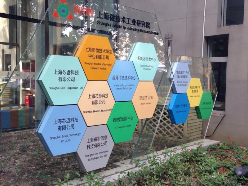
Shanghai Industrial Research Institute of Microtechnology (SIRIMT) is the first functional platform for R&D and transformation in Shanghai.
After the Municipal Science and Technology Commission validated the idea, it proposed that Shanghai should form a complete silicon-based optical interconnect chip industry chain and build a world-class silicon photonics base. Last year, silicon photonics was included in the first batch of municipal-level major special projects.
Create a complete industry chain of silicon photonics chips
Today, China's first silicon photonics R & D pilot line is under intensive construction. Last September in Shanghai Jiading District through the line of 8-inch & ldquo; beyond Moore & rdquo; R & D pilot line is part of it, the other part of the equipment is still in the procurement process. Expected this year, & ldquo; beyond Moore & rdquo; R & D pilot line of silicon photonics equipment will be put into operation. The so-called & ldquo; beyond Moore & rdquo;; refers to non-digital, diversified semiconductor technologies and products can be developed in a mature process production line, without having to follow Moore's law, that is, without having to do more and more small in the process size.
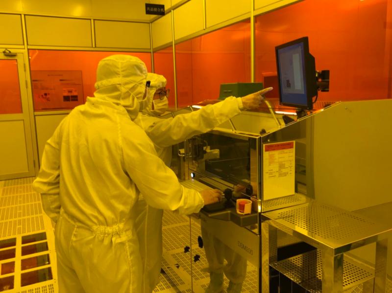
8-inch & ldquo; Beyond Moore & rdquo; R & D pilot line of the clean room, the staff in front of the machine to operate the equipment.
Time is of the essence, although some equipment is not yet in place, but Yu Mingbin has long been leading the team to develop supporting technology. “ Equipment is hardware, technology can be considered software. ” Yu Mingbin told reporters, “ in the process of buying hardware, we have to grasp the software development. So that the hardware in place, silicon photonics R & D pilot line can immediately provide services to customers. ” There is also good news that he found a partner through contacts, a process production line for the development of optical chips. This production line has flowed successfully and is serving some customers. Silicon photonics R & D pilot line through the line, Shanghai Microtechnology Industrial Research Institute will have the ability to serve a large number of customers.
Municipal Science and Technology Commission, deputy director of dry frequency, silicon photonics major special led by Zhangjiang laboratory, a number of domestic enterprises, universities and research institutes to participate in the expansion of the Shanghai Institute of Microtechnology, the R & D and transformation of functional platform functions, breakthroughs in silicon optical interconnect chip and device common key technologies, so as to attract the resources of all parties, and strive to make Shanghai become a silicon-based photonics, this strategic area of technology invention, industry, an important source of new directions. The important source of this strategic field of technology new inventions, new directions of industry.
“We want to build a whole industry chain in Shanghai, including chip design, manufacturing, packaging, testing and other links. ” Yu Mingbin said. It was revealed that the major special industry chain downstream subprojects undertaken by Shanghai enterprises have sales targets, such as Shanghai Guibo Communication Technology Co., Ltd.'s target is: to replace imported silicon photonic chips, annual sales of 100 million U.S. dollars, the cost, the process is better than traditional technology. In this regard, Guibo project team is very confident, because the global optical chip market is booming, demand exceeds supply, the current selling price of each wafer up to 15,000 U.S. dollars or more, if the mastery of the industry chain's key core technologies, there is no need to worry about market performance.
In addition to communications, optical chips can also be used for LIDAR, parallel computing, large-scale optical switching, three-dimensional optoelectronic integration and other cutting-edge projects with great development potential, and become the core components of automatic driving, a new generation of computers, ultra-high-definition television and other fields. With the advancement of the silicon photonics municipal major special project, Shanghai is expected to emerge a series of results. Wang Xi said that the special team will implement the major special project with a global vision by establishing an efficient project management mechanism, strengthening strategic planning and research, and further opening up the synergy, in order to build Shanghai into a world-class silicon photonics base at an early date.