Camera Watch 2018-12-29
On December 26, the world's first VCSEL Application Conference, organized by Mobile News Online with the theme of “VCSEL power, the trend” was successfully held in Shenzhen. Focusing on wafer-level optical chips, KunYou Photonics was invited to participate in the meeting. At the first global VCSEL Application Conference, Huang He, co-founder of KunYou Photonics, delivered a keynote speech, introducing the recent situation of KunYou Photonics and his views on the direction of industrial development to the industry leaders.
KunYou focuses on micro-optics and optical integration products, with a core team from Cambridge, Stanford and Rochester Universities, as well as Zhejiang University. Since its establishment, KunYou has received nearly 200 million RMB in financing from Walden International, Far King Capital, CSCI, KunZhong Capital, Morningside Venture Capital, ZhongHeng XingLight, Sunny Optics, and others.
The headquarter is located in Shanghai Pilot Free Trade Zone in China, which is also the sales center of KunYou Optoelectronics; the R&D center of KunYou Optoelectronics is located in the core area of Zhangjiang Hi-Tech Zone in Shanghai, which occupies an area of 600m2 with its own ultra-clean R&D center of 100,000 grade with a complete closed-loop of design, plate making, production, testing R&D and production.
And through the funding of shareholders, strategic cooperation, up to now KunYou Optoelectronics has 6-inch, 8-inch, 12-inch ultra-large-scale integrated circuits, collaboration, micro-nano optical components scale monthly production capacity of 10KK.
At the design end, KunYou Optronics uses its own algorithms and professional design software to verify and complement each other; at the plate making end, KunYou Optronics uses ebeam, laser direct writing, IC process, IBE, ICP and other processes comprehensively according to the demand; at the production end, KunYou Optronics chooses the processes of direct etching, nanoimprinting, thermal embossing, and injection molding according to the demand of materials to realize pure quartz (glass), POG, At the back-end, KUNYU Optronics uses high-precision laser cutting, automatic film expansion, and wafer-level automatic inspection equipment for efficient processing.
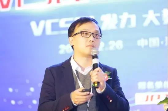
Huang He, co-founder of KunYou Optoelectronics
At the meeting, Huang He gave a detailed overview of the mass production process of KUNYU Optronics structured light DOE, TOF with diffuser, he said that the mass production process mainly covers five parts, which include determining the specification parameters, calculation simulation design, master processing and production, mass production reproduction and cutting inspection quality control, he mentioned that there is a very important link after the production is done to do the test, because it is related to the human eye It mentioned that after production, there is a very important link to do testing, because it is related to human eye safety, so now every piece of DOE will be tested.
Subsequently, according to the recent practical experience of KunYou Optoelectronics in 3D imaging product sequence, Huang He focused on summarizing and introducing the six major development trends of cell phone 3D imaging micro-nano optical product sequence in the next 2—3 years.
They are more complexity and customization of the outgoing light field Pattern; more diverse material choices, application scenarios are more subdivided; wafer size is gradually becoming larger, lithography line width is gradually becoming narrower, the scale effect is increasingly apparent; structured light and TOF bipolar outbreaks, and the continuous innovation of new design products; single-stage design to multi-stage design trade-offs, as well as process, cost trade-offs; finer process control and quality control.
Huang He said, KunYou Optoelectronics, as a link in the whole industry chain, is committed to providing customized products and services to industrial customers to cope with the increasingly complex and demanding 3D imaging product sequence.
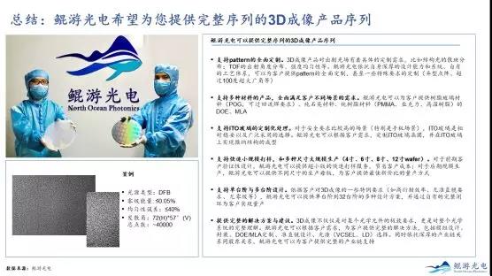
Firstly, it supports the full customization of pattern, 3D imaging products have specific customization requirements for the emitted light field, such as the scattering distribution of structured light, the angular distribution of TOF, intensity uniformity and so on. Relying on its own profound design capability and system, KunYou Photonics has its own process system, which can provide customers with full customization of patterns, and even customization of some special requirements (shaped dot matrix, more than 100 degrees of large wide-angle, etc.).
Secondly, we support a variety of materials to fully meet the needs of customers in different scenarios. KunYou can provide customers with DOE and MLA of Plexiglas material (POG, can pass the reflow soldering requirement), pure quartz material and pure resin material (PMMA, acrylic, high temperature resin).
Third, we support the customization of ITO glass. For scenes with high security requirements (especially cell phone scenes), ITO glass is a relatively stable and widely adopted choice. KunYou can customize ITO glass wafers according to customer needs and realize the molding of micro-nano structure on ITO glass.
Fourthly, we support rapid small-scale sampling, and large-scale production of multiple sizes (4-inch, 6-inch, 8-inch, 12-inch wafer). For the initial customer verification design, KUNYU can provide ultra-small version of the rapid prototyping services to save customer costs; for the later scale production, KUNYU can provide different sizes of production masters, to provide customers with better cost-effective way of mass production.
Fifth, support single-stage and multi-stage design. Based on customers' special requirements for 3D imaging (e.g. high diffraction efficiency, no collimator requirement, no zero level, etc.), KUNYO can provide a variety of design solutions from single stage to 32 stages, and realize mass production for customers through its own complete closed-loop.
Sixthly, we provide complete solutions and suggestions: 3D imaging is not only the ultimate requirement for a certain optical component, but also the complete understanding of the whole optical system. KunYou Optronics can provide customers with complete solutions according to their needs, including module design, packaging, DOE/MLA customization, collimator design, light source (VCSEL, LD) selection. At the same time, relying on the deep industrial chain relationship with shareholders, KunYou Optronics can provide customers with a complete industrial chain support.
At the end, Huang He said, KunYou Optoelectronics hopes to provide customers with comprehensive customization, and the entire sampling cycle, from customer demand, to complete the design of a publication, about three to five days, within two weeks to provide customers with the first batch of samples, iteration cycle is very fast, samples, the effect of the determination, and then spend three or four weeks of preparation time, can be given to the customer for batch production. In addition to DOE and device provision, KunYou can also provide program support according to customer needs.