Mobile News Online Camera Watch
At present, wafer-level optical technology makes a series of new cutting-edge needs possible, including 3D imaging and face recognition, AR/MR, 5G optical communication, intelligent industry and so on. Even some of the popular & ldquo; electric & rdquo; field, perhaps also can use wafer-level optics ideas another way.
In this & ldquo; soft and hard & lsquo; ingestion & rsquo;, listen & middot; see AI & rdquo; 2018 Chongqing International AI Phone Industry and Technology Summit, Dr. Tao Lin, chairman of the board of directors of KunYou Optoelectronics, brought a keynote speech, "Discussing the development trend of DOE/Diffuser for 3D Sensing".
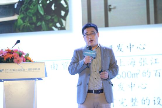
Lin Tao, Chairman of Kunyou Optoelectronics
KunYou Optoelectronics is a high-tech enterprise specializing in the field of micro-optics and optical integration, headquartered in Shanghai, China. The company is composed of top international and domestic scholars in the field of optoelectronics and industry veterans with many years of experience in the optoelectronics industry. The core R&D team and management include professors and PhDs from Stanford University, University of Rochester, University of Cambridge, Zhejiang University, Shanghai Jiaotong University and other well-known optoelectronic institutions; former executives from Microsoft, NASA, Fortis Fiber Optics, Horizon Semiconductor, McKinsey and other internationally renowned companies. Members of the core R&D team have been awarded the Second Prize of National Scientific and Technological Progress, National May 1st Labor Medal, and so on. Relying on its own profound technical accumulation and unique manufacturing process, KunYou Optoelectronics is able to provide one-stop design, customization, and production of precision micro-optical products and services for domestic and foreign customers at an unparalleled cost-effective price. Since its establishment, the company has received nearly 200 million RMB in financing from Walden International, Far King Capital, CSCI, KunZhong Capital, Morning Glory Venture Capital, Zhongheng Xingguang, Sunny Optics, and others.
On the scene, Dr. Tao Lin, based on the recent practical experience of KunYou Optronics in 3D imaging product sequence, focused on summarizing and introducing the six major development trends of cell phone 3D imaging micro-nano optics product sequence (DOE, Diffuser) in the next 2-3 years, which are as follows: 1. The outgoing optical field Pattern is more complex and customized; 2. The material choices are more diversified, and the application scenarios are more subdivided; 3, Gradually larger wafer size, lithography line width gradually become narrower, the scale effect is increasingly apparent; 4, structured light and TOF bipolar outbreak, and the continuous innovation of new design products; 5, single-stage design to multi-stage design trade-offs, as well as process, cost trade-offs; 6, more sophisticated process control and quality control.
Dr. Tao Lin said, KunYou Optoelectronics, as a link in the basic layer of the whole industry chain, is committed to providing customized products and services for industrial customers to cope with the increasingly complex and demanding 3D imaging product sequence. Specifically including:
1. Supporting full customization of patterns, 3D imaging products have specific customization requirements for the emitted light field, such as the scattering distribution of structured light, the angular distribution of TOF, intensity uniformity and so on. Relying on its own profound design capability and system, KunYou Optronics can provide customers with full customization of patterns and even some special requirements (shaped dot matrix, over 100 degrees wide-angle, etc.).
2. Support a variety of material products, to fully meet the needs of customers in different scenarios. KunYou can provide customers with resin-glass material (POG, can pass the reflow requirement), pure quartz material, pure resin material (PMMA, acrylic, etc.) DOE, MLA.
3. Support customized processing of ITO glass. For scenes with high security requirements (especially cell phone scenes), ITO glass is a relatively stable and widely adopted choice. KunYou can customize ITO glass wafers according to customers' needs and realize the molding of micro-nano structure on ITO glass.
4. Support rapid small-scale prototyping, and large-scale production of multiple sizes (4-inch, 6-inch, 8-inch, 12-inch wafer). For the initial customer verification design, KUNYU can provide ultra-small version of the rapid prototyping services to save customer costs; for the later scale production, KUNYU can provide different sizes of production masters, to provide customers with better cost-effective way of mass production.
5. Support single-stage and multi-stage design. Based on customers' special requirements for 3D imaging (e.g., high diffraction efficiency, no collimator, no zero level, etc.), KUNYO can provide a variety of design solutions from single-stage to 32-stage, and realize mass production for customers through its own complete closed-loop.
At the end, Dr. Tao Lin said that 3D imaging is not only the extreme requirement for a certain optical component, but also the complete understanding of the whole optical system. KunYou Optronics can provide customers with complete solutions according to their needs, including module design, packaging, DOE/MLA customization, collimator design, and light source (VCSEL, LD) selection. Relying on the deep industry chain relationship and shareholders, KUNYU can provide customers with a complete industry chain support.