
With the new generation of iPhone X importing front structured light solution to achieve 3D imaging, making it the new standard for smartphones, 3D imaging in cell phones and non-mobile phones will usher in a major outbreak. Ordinary camera to achieve 2D plane imaging, lost the physical world of the third dimension information (size and distance and other geometric data), the computer can only achieve image recording and plane image feature recognition, analysis algorithms are extremely difficult to realize the intelligent analysis of the current function is very limited. 3D imaging can identify the field of view of the space of the space of each point of the three-dimensional coordinate information, so that the computer to get the space of the 3D data and can recover the complete three-dimensional world and realize a variety of intelligent analysis function. This enables computers to obtain 3D data in space and recover the complete 3D world and realize all kinds of intelligent 3D positioning.
As an important product in the field of micro-nano optics, KUNYU Optronics has already mass-produced and fully supplied products for 3D imaging to customers:
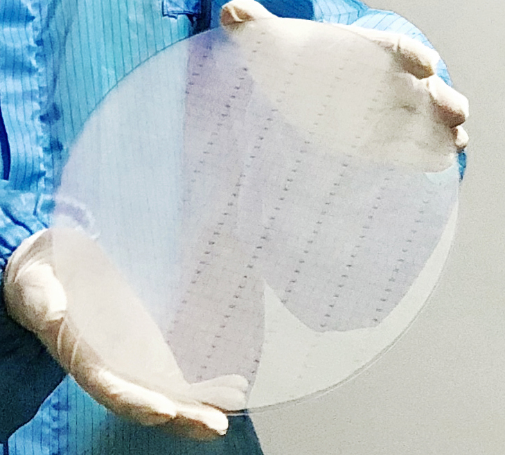
KUNYU Optronics mass production type complete 8-inch full-sub DOE wafers (Yield >97.5%) |  Scattered structured light DOE based on single-point LDs |  基于VCSEL阵列的Diffuser |
 Neat splicing DOE based on VCSEL arrays | 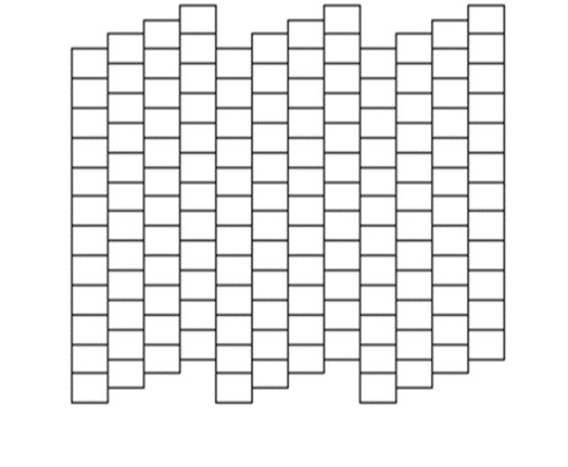 Misaligned splicing DOE based on VCSEL arrays |
KunYou's 3D imaging product sequence has several advantages. 1:
1. Supporting full customization of patterns, 3D imaging products have specific customization requirements for the emitted light field, such as the scattering distribution of structured light, the angular distribution of TOF, intensity uniformity and so on. Relying on its own profound design capability and system, and its own process system, KunYou Optronics can provide customers with full customization of patterns, and even some special requirements (shaped dot matrix, more than 100 degrees of large wide-angle, etc.).
2. Support a variety of material products, to fully meet the needs of customers in different scenarios. KunYou Optoelectronics can provide customers with Plexiglas material (POG, can be over the reflow soldering requirements), pure quartz material, pure resin material (PMMA, acrylic) DOE, MLA
3. Support customized processing of ITO glass. For scenes with high security requirements (especially cell phone scenes), ITO glass is a relatively stable and widely used choice. KunYou can customize ITO glass wafers according to customers' needs and realize the molding of micro-nanostructures on ITO glass.
4. Support rapid small-scale prototyping, and large-scale production of multiple sizes (4", 6", 8", 12" wafer). For the early stage of customer's verification design, KUNYO can provide ultra-small version of rapid prototyping services to save customers' costs; for the later stage of large-scale production, KUNYO can provide different sizes of production masters, to provide customers with better cost-effective way of mass production.
5. Support single-stage and multi-stage design. Based on customers' special requirements for 3D imaging (e.g. high diffraction efficiency, no collimator, no zero level, etc.), KUNYO can provide single-stage to 32-stage design solutions, and realize mass production for customers through its own complete closed loop.
6. Provide complete solutions and suggestions: 3D imaging is not only about the extreme requirements of a certain optical component, but also about the complete understanding of the whole optical system. KunYou Optronics can provide customers with complete solutions according to their needs, including module design, packaging, DOE/MLA customization, collimator design, and light source (VCSEL, LD) selection. Relying on the deep industry chain relationship and shareholders, KunYou can provide customers with a complete industry chain support.
Welcome to contact us for more information!